Since integrating ADCs and their improved versions have been the most widely used ADC type in digital multimeters and voltmeters over the past fifty years, this article documents the process of designing an integrating ADC.
Time and frequency are the earliest, most widely used, and most accurate physical quantities measured by humankind. As early as 1820, 150 years before Ampère invented the first galvanometer, Huygens invented the first pendulum clock. Even now, top-of-the-line digital multimeters costing tens of thousands of yuan, such as the HP3458A, have a measurement resolution of only 8 1/2 digits, while frequency meters costing a thousand yuan, such as the HP53132A, can achieve a measurement resolution of 12 3/4 digits. Therefore, converting physical quantities such as voltage and current into time for measurement can greatly reduce system complexity and introduced errors.
In fact, the most accurate voltage references today are based on frequency/voltage conversion: passing microwaves through a weak point sandwiched between two superconductors (separated by an insulating/non-superconducting material), this produces an extremely stable and precise DC voltage due to the inverse Josephson effect.
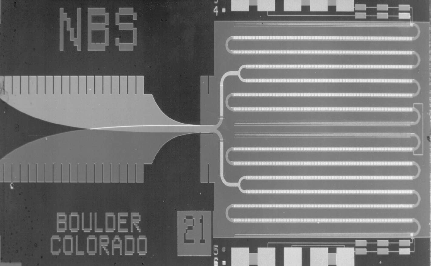
The image shows a Josephson DC voltage reference chip manufactured by NIST, with 3020 nodes, used to generate a 1V voltage, requiring liquid helium cooling during operation.
To convert voltage to time, we need to construct a voltage function related to time. In the basic circuits, it’s clear that the response of the basic four arithmetic units does not include time, and the DC response of the filter is non-linear, leaving only the differentiator and integrator as options. Since we are actually only concerned with the DC signal, a capacitor integrator is chosen to construct the V/T conversion core of the ADC. A capacitor is chosen instead of an inductor because inductorance is difficult to control.
Basic form of an integrator TI.com
The transfer function of an ideal integrator is:
If we set a voltage
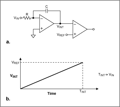
Single-slope integrator ADC architecture Analog.com
However, this architecture is highly dependent on the absolute values of the two passive components
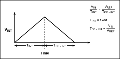
Double-slope integral ADC,来源:Analog.com
Therefore,
If
This scales
Improved (Dual-Slope) Dual-Ramp Integrator ADC, Source: p.4, April 1989, HP Journal 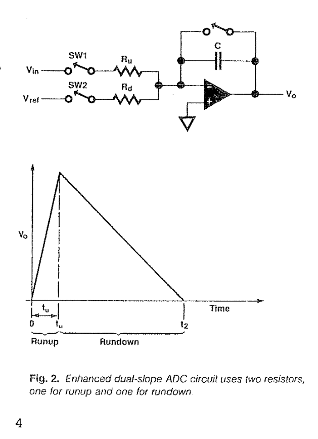
However, dual-ramp integrators have significant drawbacks:
-
Real-world integrators are limited by the power supply rails and cannot integrate indefinitely to positive or negative infinity. Furthermore, comparator offset requires us to utilize the full dynamic range of the integrator as much as possible (obviously, the error caused by offset is the ratio of the integrator’s full-swing voltage to the offset voltage). Therefore, the integration time of this type of ADC is very fixed and inflexible. For example, the AC power grid in laboratories often causes severe power frequency interference, and the frequencies of global power grids are not entirely the same. This requires our input integration time to be an integer multiple of the power line cycle (abbreviated as NPLC, Number of Power Line Cycle). For a 60Hz power grid, this is 16.67ms, while for a 50Hz power grid, it is 20ms. To prevent the integrator from saturating, we must design the integrator’s time constant according to 50Hz. Since the dynamic range of the integrator cannot be fully utilized, this will lead to a loss of accuracy for the instrument under a 60Hz power grid! Furthermore, benchtop multimeters in laboratories often face various operating conditions, and we cannot always expect the instrument to operate at maximum resolution—often 10NPLC or higher, especially since ultra-high precision measurements are not common in laboratories.
-
Larger resistance and capacitance values are difficult to manufacture, and their electrical characteristics are worse than smaller models. To achieve an integration time of 20ms,
would be 0.02. This value may not seem large, but considering that the largest common option for a C0G capacitor in a 1206 form factor is 100nF, this would require a 200kΩ input resistor. On one hand, high impedance sources within the instrument are undesirable, causing excessive picking up of ambient noise and severely degrading performance. On the other hand, reducing the resistance and increasing the capacitance would result in a very large capacitor to achieve (or even fail to achieve) excellent electrical characteristics, leading to higher leakage current.
While we could fabricate resistors in multiple proportions and execute the two ramps at different slopes to create a multi-slope dual-slope integrator ADC, designing a high dynamic range integrator remains very challenging as described above (in fact, excessively large or small slopes will severely affect the linearity of the integrator output stage and produce uneven heating in the resistor array). Integrating resistors that differ by several orders of magnitude and ensuring they do not interfere with each other is also costly.
Therefore, to address manufacturing challenges and achieve a more flexible operating range, we adopted a smaller integrator time constant to obtain a smaller passive component size. During RunUp, a switch is used to toggle between
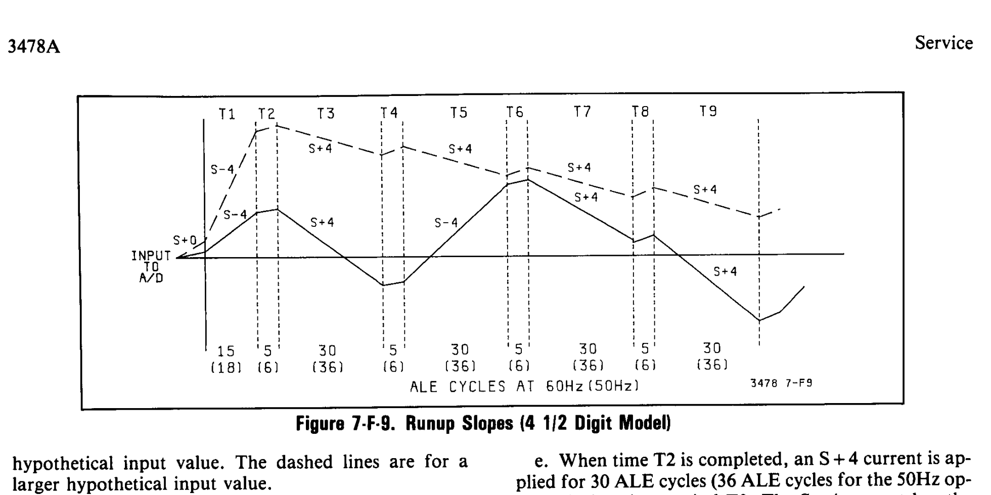
HP3478A Dual-Slope Multi-Ramp RunUp Process 3478A DMM Service Manual
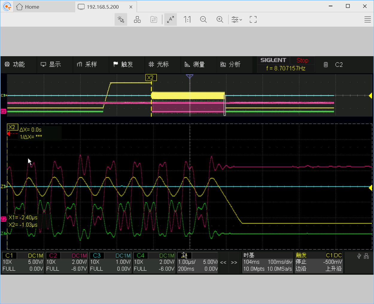
Due to the charge injection effect and switching nonlinearity of MOSFETs, we must use a well-designed switching sequence during switching to ensure a constant and symmetrical number of MOSFET switching operations. Symmetrical switching within a switching mode helps eliminate charge injection and reduce offset, while a fixed number of switching operations within a switching mode will generate a fixed nonlinear offset, which can be calibrated later. This will generate a waveform approximating PWM, as shown below:
Switch sequence, Source: p.7, April 1989, HP Journal 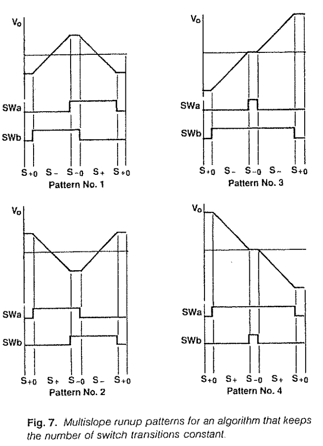
After the majority of the RunUp time has ended,
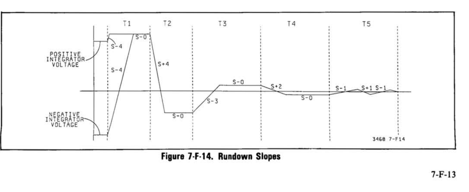
HP3478A multi-slope multi-ramp RunDown process 3478A DMM Service Manual
Furthermore, since
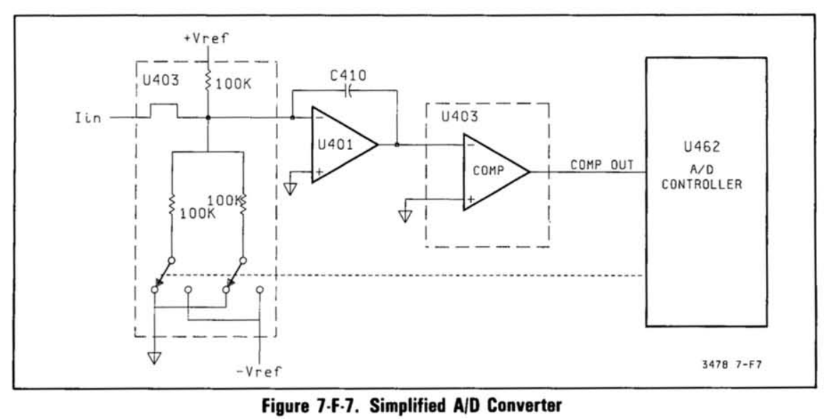
Simplified ADC diagram of HP3478A 3478A DMM Service Manual
Based on this, the prototype of the HP Integrating ADC II was completed. The 3456A, 3457A, 3458A, 3468A, and 3478A all used different variants of the second-generation HP Integrating ADC. We will not go into the specific implementation details of each one. With subsequent advancements in semiconductor technology, the 34401A replaced the RunDown stage with an ADC and continuously executed RunUp, measuring the integrator voltage before and after each cycle, achieving faster, almost uninterrupted sampling. The 34410A further replaced the comparator directly with an ADC and used a newer MOSFET switch to significantly improve RunUp resolution. The newer ADC also improved RunDown accuracy, thereby achieving a sampling speed an order of magnitude higher than the 34401A. As for the newer 3446x series, the author has not yet had access to a physical device, so it will not be discussed.
Prototype
Multislope v1
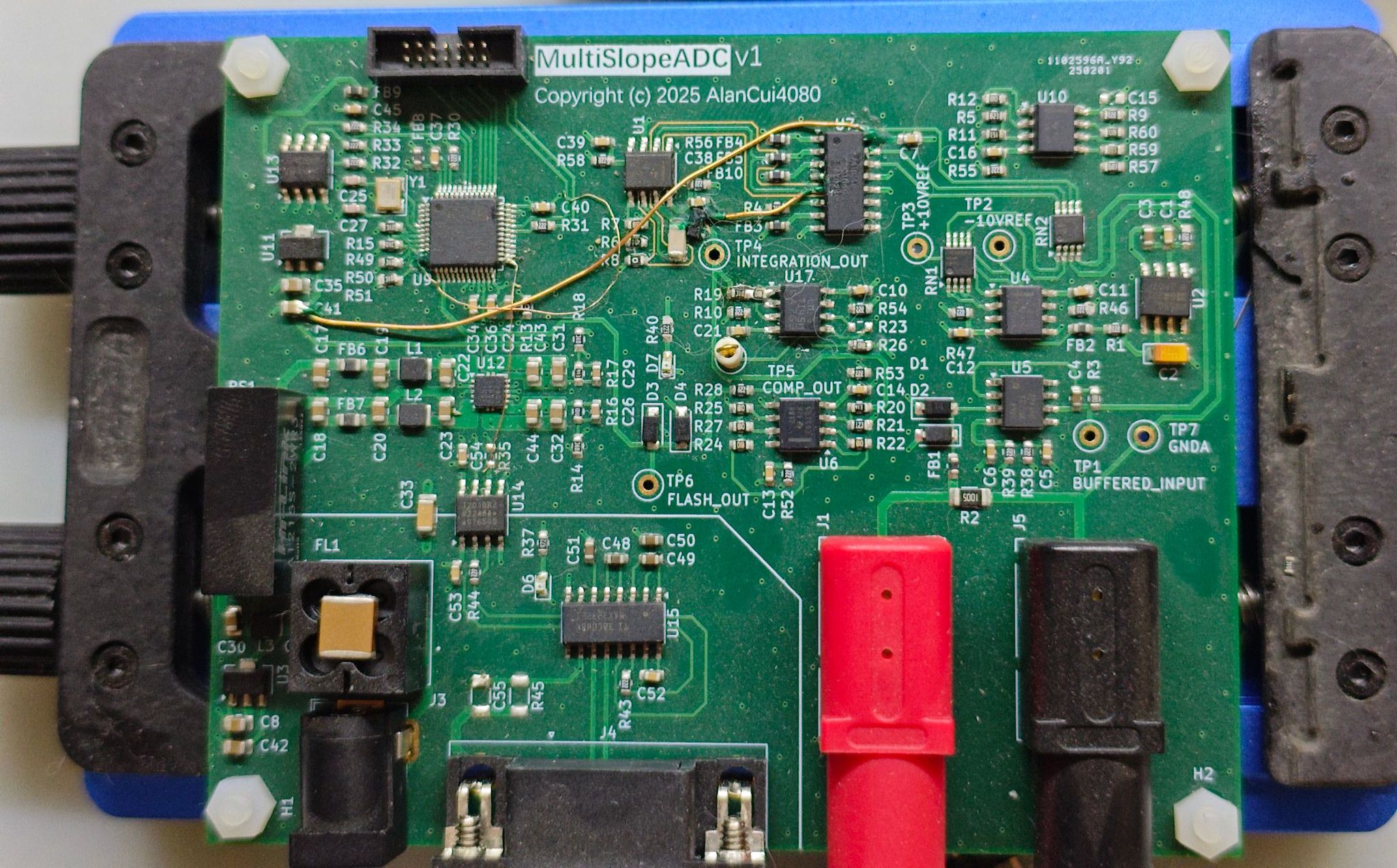
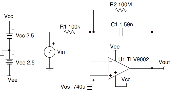
The Alan multi-slope ADCv1 is largely modeled after the HP34401A, controlled by an STM32 hardware timer, and uses an ADR4550 and LT5400 resistor network to generate a ±10V reference. The integrator uses an LT5400 resistor network as the input and a 74HC4053 as the switch. When the 4053 switch is not connected, current is diverted to GND to prevent the voltage across the switch from exceeding its withstand voltage. When connected, due to the op-amp’s closed-loop design, the inverting input is also connected to GND. The power supply section uses a combination of Mornsun positive and negative isolation modules, multiple filters, and a TPS7A39.
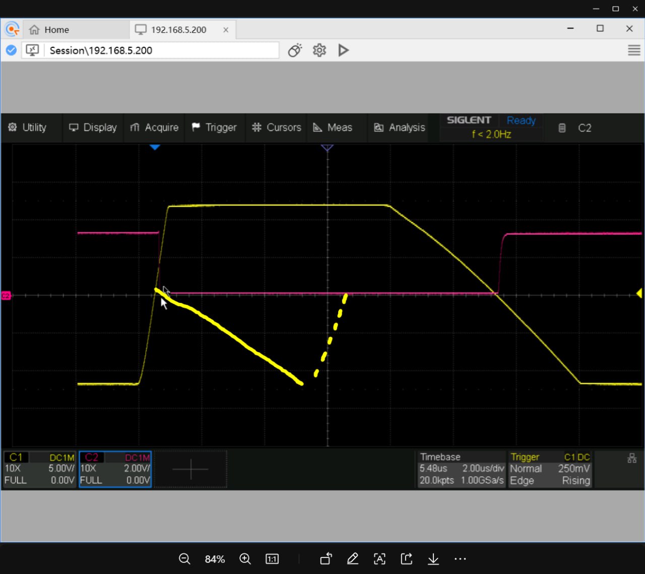
This schematic has several issues. For example, the LM311’s input stage slew rate is low, resulting in significant latency. Therefore, a resistor divider is needed to limit the input stage voltage to a lower slew rate; see TI E2E. Secondly, the 1nF+1k RC combination is too small, causing the STM32 interrupt to reach the GPIO pin too slowly, resulting in the integrator saturating (see the diagram above) and becoming completely inoperable. Additionally, the output FLASH ADC transfer circuit is overly complex.
Multislope v3
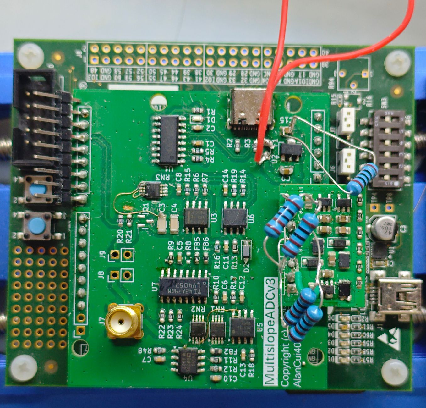
The Alan multi-slope ADCv3 largely mimics the HP34401A, controlled by a MAX10 10M08 FPGA. The core is the same as v1, but the FLASH ADC is removed, and the comparator is replaced with a TLV3202. The power supply uses a self-made SEPIC+CUK+post-LDO. The board design is a modified MAX10 EVAL Arudino-style expansion board. The main issue with this board was an abnormal wiring of the LT5400 series resistor array, which was resolved by jumper wires.
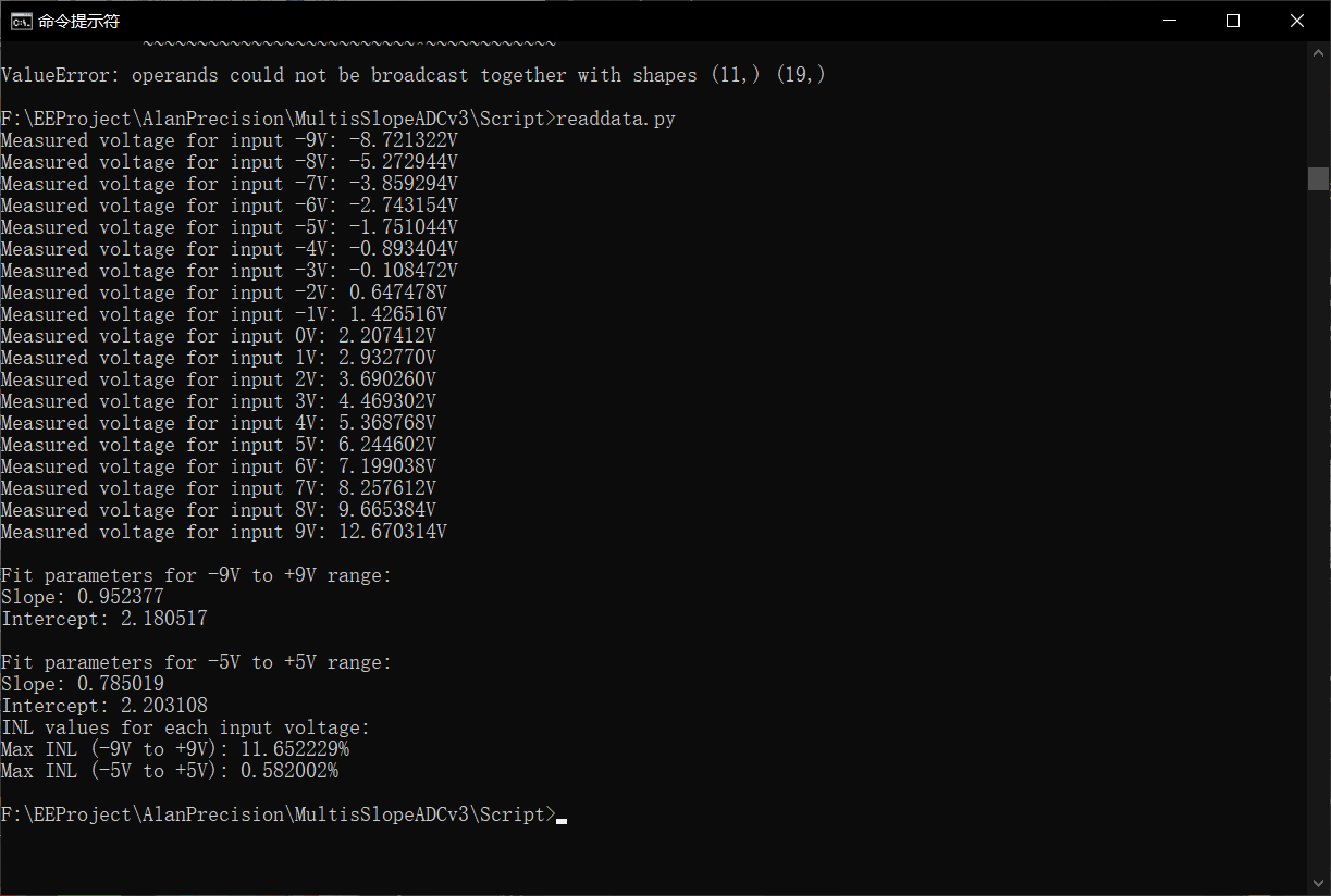
Using conventional bang-bang control, this board successfully achieved 4-bit resolution with a 10NPLC, with a maximum INL of 0.58% without using MOSFETs to mitigate non-ideal switching modes. The converter sends binary data via serial port after each conversion. The following is the result of decoding and calculating the INL using a Python script:
SourceCode: https://github.com/AlanCui4080/MultiSlopeADCv3