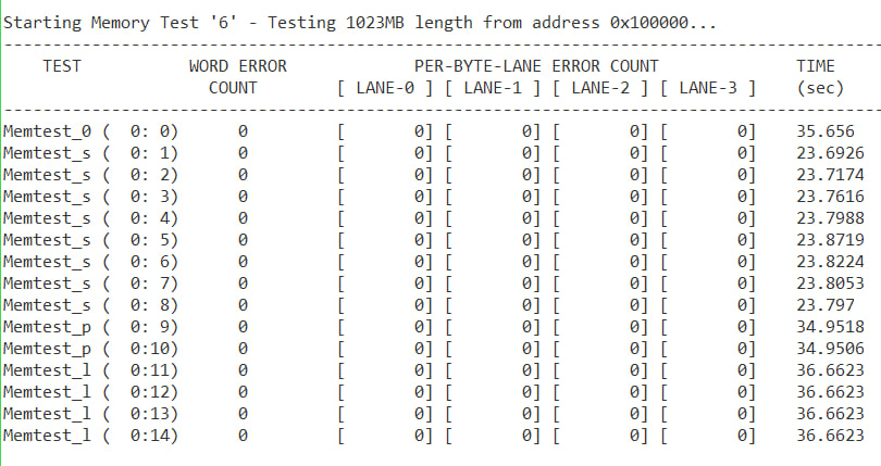
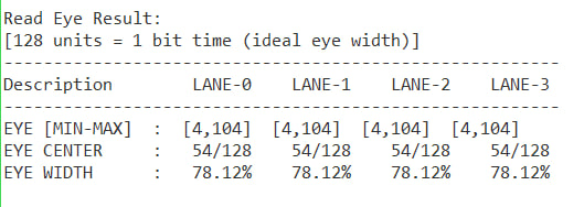
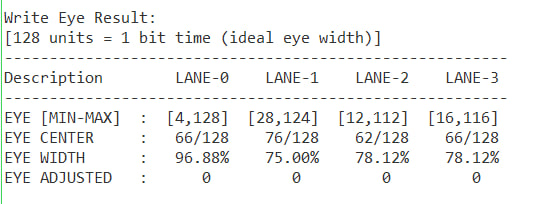
Two and a half years ago, I drew my first flyby ddr3 memory layout when I first came into contact with high-speed PCBs. Later, although I have debugged many DDR3/DDR4 designs, I never tested this board that was already assembled. One reason is that the JTAG pin headers reserved are 1.27mm, making debugging inconvenient. Another reason is that this hardware needs several modifications to run normally. Finally, I got around to testing it, and here are the results: