With the increasing number of time and frequency instruments in the laboratory, the two 10MHz reference outputs built into the GNSSDO are no longer sufficient for simultaneous operation. Therefore, a 1:8 10MHz clock distribution amplifier was designed and fabricated. Thanks to @滚筒洗衣机 for soldering most of the circuitry; this design is partly derived from the SRS FS730.
Design
The input is filtered by a low-pass filter. The main amplifier uses an OPA690 (GBW=535MHz) configured with G~=18V/V (to ensure a bandwidth of at least 30MHz). Part of the output is fed to the input detector for the input validity indicator, and the other part is output to a fly-by distributing bus, AC terminated at the end, then fed into an OPA365 with G=2 for output buffering. An elliptic filter is connected at the output. This filter is designed to have its first stopband dip at 20MHz, with a designed -3dB point of approximately 11.2MHz, effectively attenuating harmonic components caused by saturation (clipping at the rail). This amplifier exhibits input-output delays between different channels due to its fly-by distributing bus configuration.
After amplification, signals exceeding 0dBm are amplified to rail-to-rail voltage (9Vpp), attenuated to 4.5Vpp by R70-R71, and finally 2.25Vpp on a properly terminated distributing bus. The output stage amplifier (G=2) then amplifies the signal to 4.5Vpp@HiZ or 2.25Vpp@50Ω (approximately 11dBm). This value can be corrected to approximately 10dBm by adjusting R71 or reduced to 4dBm by shorting the option jumper at output amplifier.
DistrubutionAmplifierv1Schematic
Testing
The amplifier consumes 322mA@5V under no-load conditions and 392mA@5V with a +20dBm input. The input design power is +20dBm, and it did not fail during testing at +23dBm.
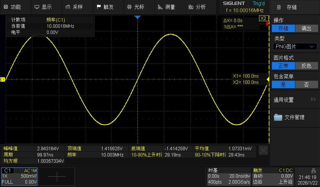
The following tests were conducted with a +3dBm input:
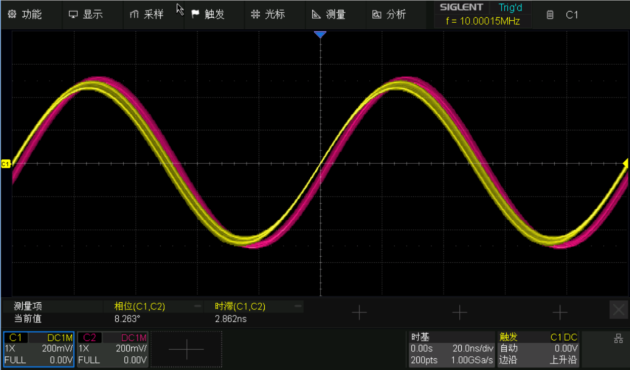
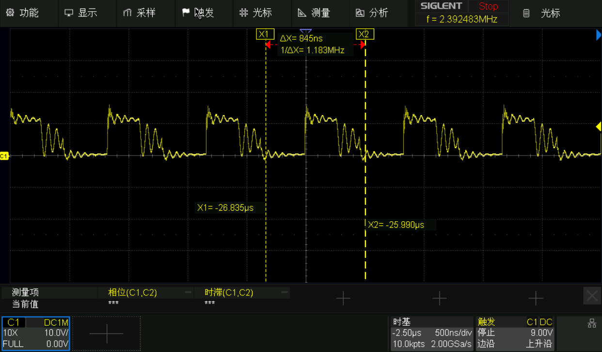
- First and last channel output delay is 2.862ns or 8.263°
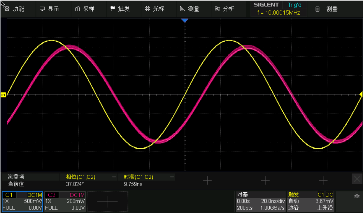
- Input to the last channel delay was 9.759ns or 37.024°
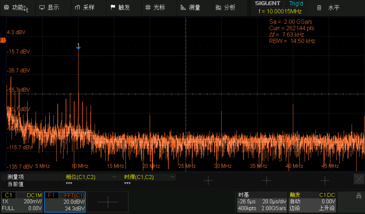
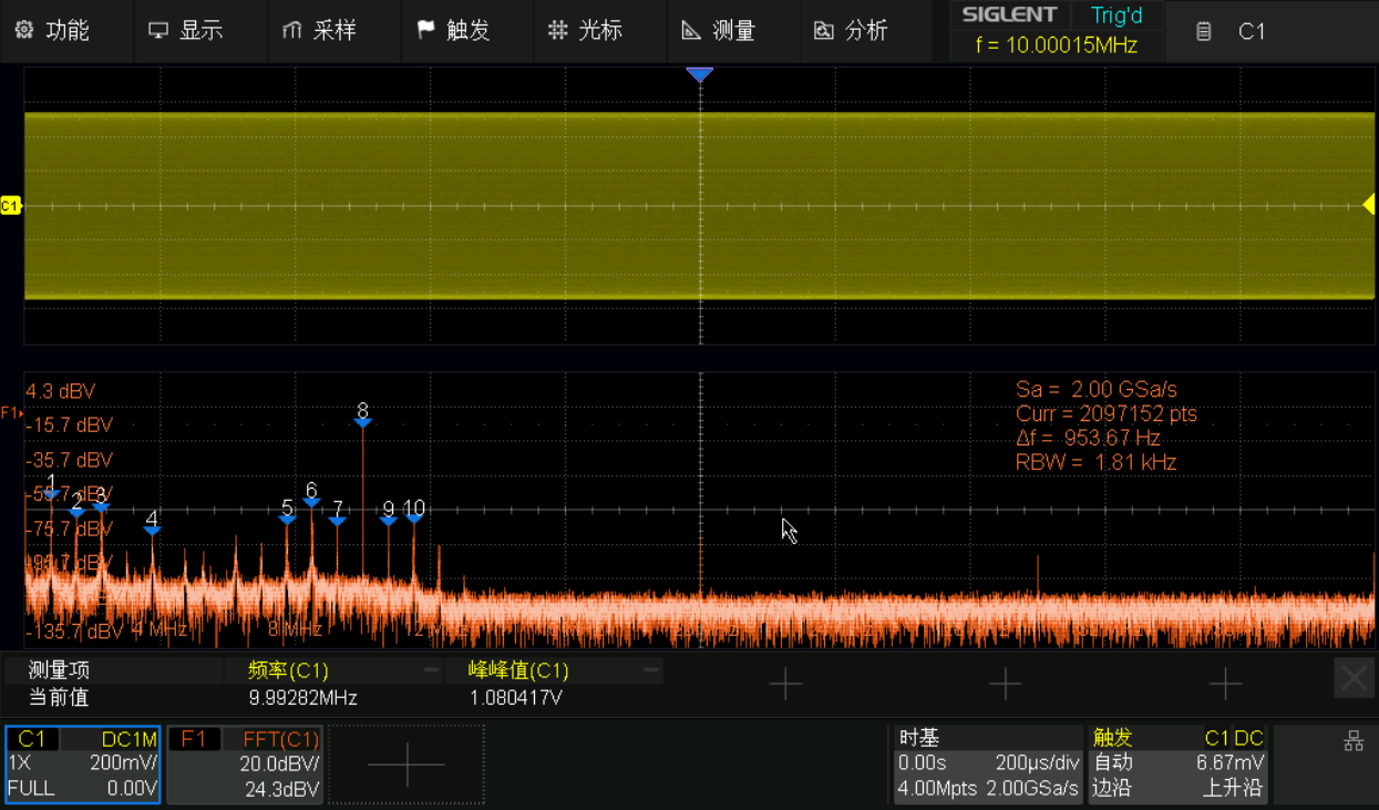
- First and second harmonics of output are < -60dBc, and the third harmonic is approximately -60dBc, demonstrating the excellent characteristics of the output filter.
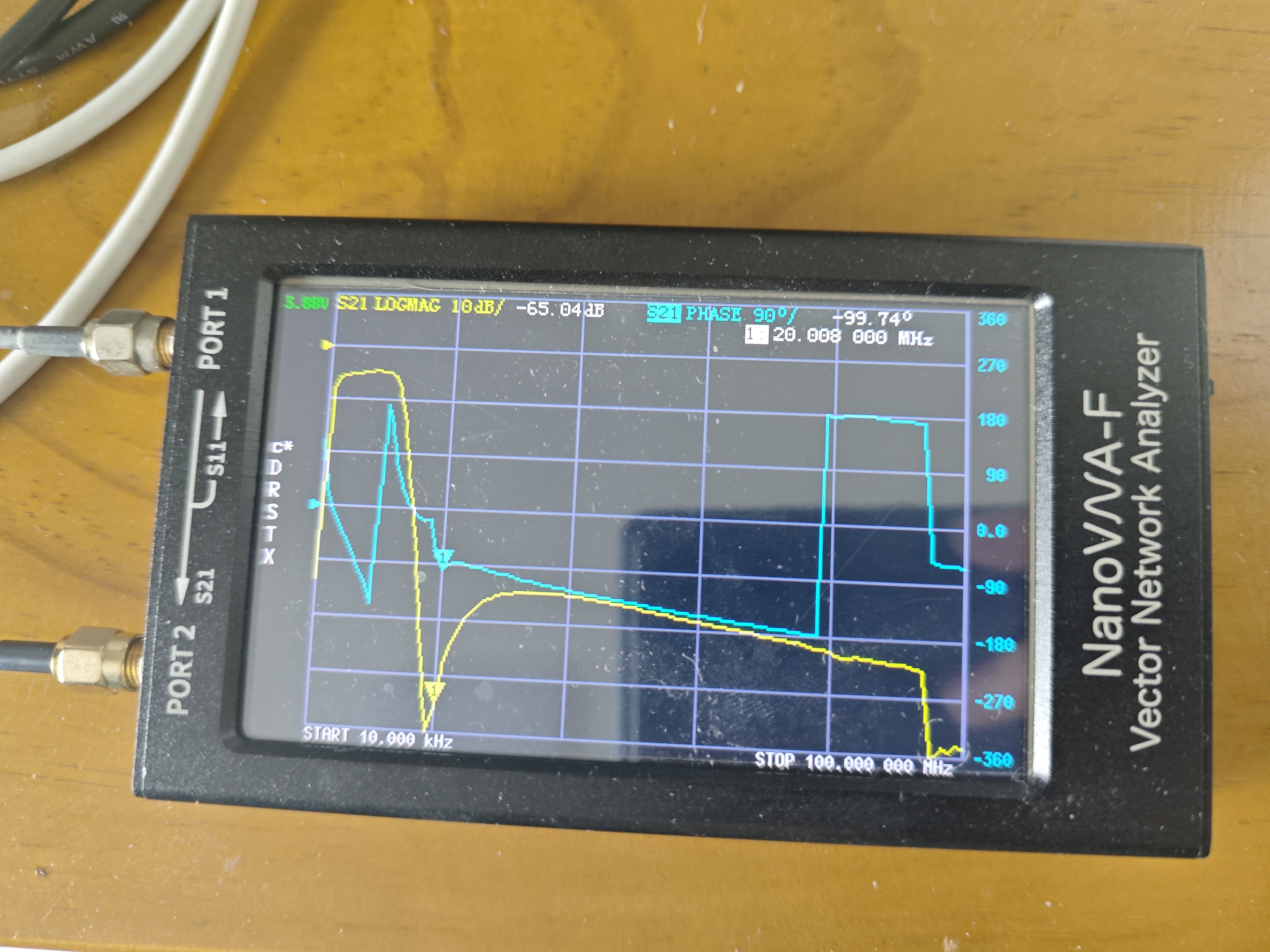
Actual measurements confirm that the filter attenuates to -65.04dB at the second harmonic, only 10dB higher the theoretical value.
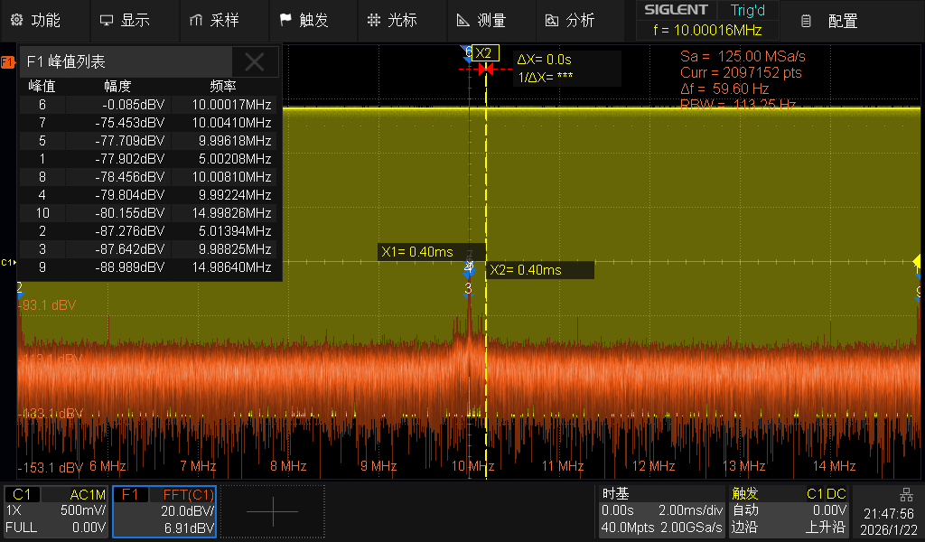
However, as shown in the figure, the switching frequency of the SEPIC-Cuk converter in DCM mode mixes with the output frequency, resulting in a cluttered output spectrum. However, none of the components exceed -40dBc and are approximately 500kHz from the center frequency, sufficient for selection using a bandpass filter. But a more critical issue is the output stage buffer OPA365’s slew rate of only 25 V/µs (measured at 28.9V/µs), requiring 125.66V/µs to output 2Vpp at 10MHz. While the output filter is robust enough to reconstruct the waveform, the amplifier is still insufficient for the output stage, resulting in an excessively low output amplitude. In addition, the input stage is DC-coupled. Due to the high performance of the input amplifier, the input stage is unlikely to be fully loaded and cause problems, but this will reduce the robustness of the overall system.
Fix up
Replacing the OPA690 with the TPH2501 alleviated the slew rate issue and reduced output jitter, resulting in a standard output level of 1Vrms. Additionally, the TPH2501 appears to have overvoltage protection, automatically protecting itself at ±5V, causing the input current to drop to 100mA. Modifying the voltage to ±3.7V resolved this, restoring the input current to approximately 170mA.